
Fabrication Process Details
See below for alignment marks and mask layouts.
| Wafer Cross-Section | Step | Notes/Details |
|
|
(1) RCA clean standard <100> 6" Si wafer |
oxidation recipe "4W1000" details: take wafers straight to coater track after diffusion tube
|
| (2) deposit 300-400nm thermal SiO2 machine: (ICL tube) 5D-ThickOx |
||
 after Step (3) |
(3) photolithography: Mask 1 – "KOH TIPS" machines: coater6 (ICL), EV1 (TRL) |
coater6: 1.2um recipe using SPR700 resist (2000RPM spin for 30 sec. gives 1.2um) EV1: 2.0 sec. exposure |
 after Step (4) |
(4) etch windows in oxide - ~5 min. BOE |
(last run did 4.5 min. BOE, then 10 min. piranha resist strip) |
 after Step (5) |
(5) etch Si pits in KOH (depth ~15-20um),
~30min. machine: ***KOH bath (Manalis Lab)*** |
|
 after Step (6) |
(6) post-KOH clean & oxide strip: 1. double piranha clean -- 10 min. in yellow-dot fabware -- then 10 min. in green-dot fabware 2. ~6 min. BOE in green-dot fabware (cleans + strips oxide) machine: acid-hood (TRL) |
|
 after Step (8) |
(7) RCA clean to prepare for SiNx deposition machine: rca-ICL (ICL) |
|
| (8) deposit 800nm low-stress SiNx machine: VTR (ICL) |
measure nitride film thickness using UV1280 on five wafers spread throughout lot -- need ave. and range | |
 after Step (9) |
(9) photolithography: |
HMDS: thumbwheel at 4 exposure: 3 sec. & use hard contact to make sure fingers come out develop: 1 min. 15 sec. |
 after Step (10) |
(10) etch silicon nitride, front and back then strip resist machine: AME5000, Chamber A (ICL), asher (ICL) |
recipe: NITRIDE CF4 etch rates: time to clear (from prev. run): |
| start 6" Pyrex wafer - ALL PROCESSING AFTER THIS IS RED-DOT | ||
|
after Step (11) |
(11) photolithography: Mask 3 – "GLASS ETCH" machine: coater, EV1 (TRL) |
|
|
after Step (12) |
(12) etch Pyrex (2-3um deep) 20-30min. BOE then strip resist - 10 min. piranha machine: acid-hood (TRL) |
(BOE may be too slow and resist may lift off too much in the 20-30 min. necessary) good alternative may be Water/HF/Nitric Acid mixture, in ratio of 65%, 20%, 15% (Pyrex etch rate approx. 0.8um/min) |
|
after Step (13) |
(13) coat both sides of Pyrex with 3um thick resist to protect
during diesawing machine: coater (TRL) |
pre-bake only, no need to postbake -- easier removal after diesawing done |
|
after Step (14) |
(14) diesaw wide lanes in Pyrex ~300um
deep machine: diesaw (ICL) |
use special 1mm extra wide blade - Disco: P1A862 SDC320N50BR50 56x1.0x40 |
|
after Step (16) |
(15) strip protective resist with acetone in red-dot solvent
beaker machine: photo-wet-Au (TRL) |
use dirtiest red-dot beaker you can find |
| (16) double piranha clean after diesaw machine: acid-hood (TRL) |
||
|
after Step (17) |
(17) align and anodically bond Pyrex and
Si wafers machine: EV501-620 (TRL) |
need to do piranha before bonding each pair of wafers |
|
after Step (18) |
(18) saw borders of device dies, leaving 20-50um of glass uncut |
|
|
after Step (19) |
(19) release cantilevers by dissolving
bulk Si machine: ***KOH bath (Manalis Lab)*** |
|


Alignment Marks
|
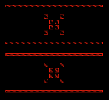
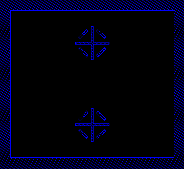
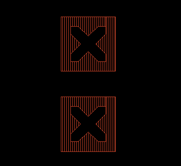
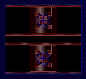
Mask 1: KOH TIPS |
Mask 2: SIN FRONT
|
 |
 |
|
Mask 3: GLASS ETCH
|
All masks superimposed
|
 |
 |